Photonic Integrated Beamlines for 3D Magneto-Optical Trap
US20240203616
2024-06-20
Physics
G21K1/003
Inventors:
Assignee:
Applicant:
Drawings (4 of 13)


Smart overview of the Invention
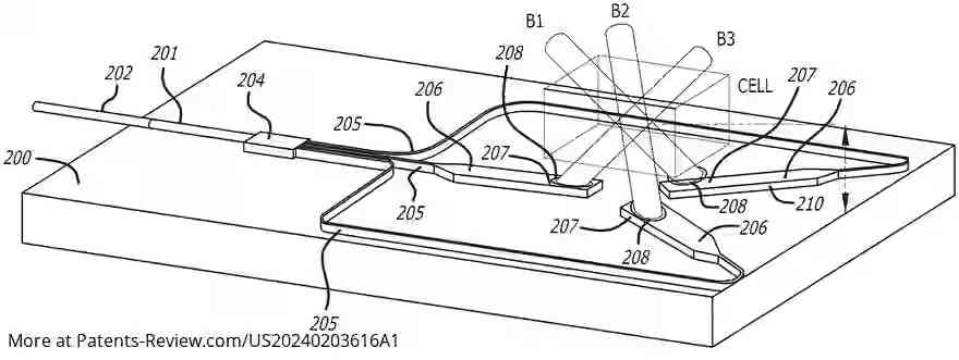
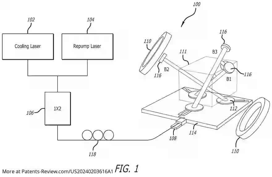
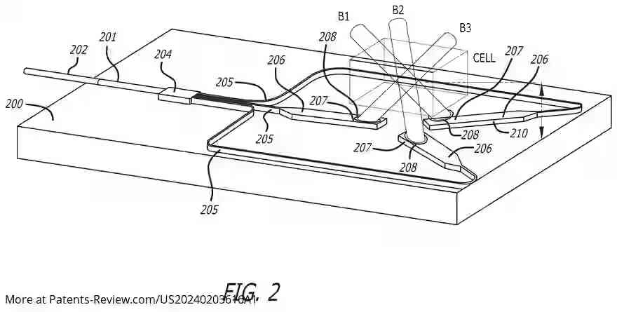
A photonic integrated circuit is designed to enhance the functionality of an atomic cell, specifically for applications in 3D magneto-optical traps (3D-MOTs). The circuit includes a set of three grating emitters arranged around the circumference of the circuit, spaced approximately 120 degrees apart. Each emitter is precisely etched to direct beams at specific angles onto the atomic cell's first wall, ensuring that the emitted beams converge at a designated point within the cell.
Applications of 3D Magneto-Optical Traps
3D-MOTs play a crucial role in producing cold atoms, which are essential for precision applications such as atomic clocks, spectroscopy, and quantum information sciences. These traps utilize laser cooling and magnetic fields to capture and stabilize neutral atoms. The configuration allows for multiple laser beams to intersect within the trap, creating a controlled environment for manipulating atomic states.
Photonic Integrated Circuit Features
- Incorporates at least one laser stabilized to a frequency reference.
- Includes photodiodes and feedback control circuits for precise locking of laser frequencies.
- Utilizes output coupling gratings that can form optical tweezers or lattice traps.
- Compatible with various atomic species and configurations, including ion traps and molecular traps.
Integration and Manufacturing
The photonic integrated circuit is designed to be compatible with CMOS manufacturing processes, utilizing materials such as silicon nitride. This integration allows for efficient coupling and delivery of laser beams while maintaining stability and precision. Additional components like repump and cooling lasers can also be integrated into the circuit to enhance its functionality.
Advancements in Atomic Manipulation
The integration of photonic circuits into 3D-MOTs represents a significant advancement over traditional bulk-optic technologies. By reducing size, weight, and cost while improving performance stability, these circuits facilitate more sophisticated experiments involving cold atoms, ions, and molecules. This technology opens new avenues for research in areas such as Bose-Einstein condensates and atom interferometry.