NON-VOLATILE MEMORY CELL STRUCTURES AND METHODS OF MANUFACTURING THEREOF
US20240257874
2024-08-01
Physics
G11C16/0483
Inventors:
Assignee:
Applicant:
Drawings (4 of 9)


Smart overview of the Invention
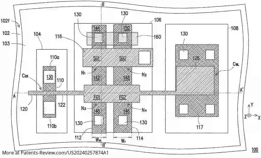
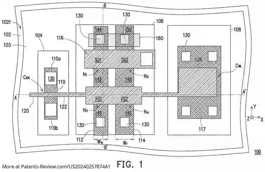
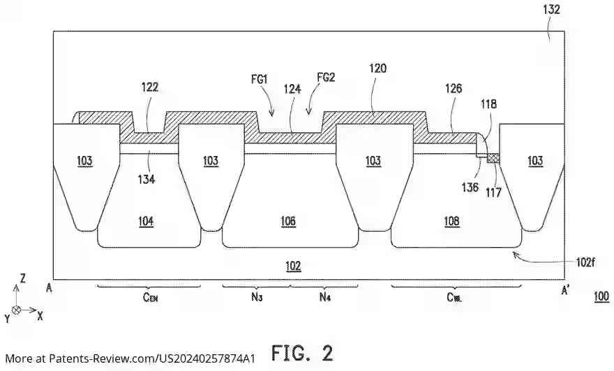
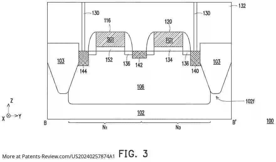
A memory device is designed with multiple well regions, including a first, second, and third well region. The second well region is positioned between the first and third regions, with the third regions being separated from each other. Floating gates are placed over these well regions, extending continuously from the first to the corresponding third region. The device also features distinct bit line write and read regions located within the second well region, each containing source/drain regions adjacent to the floating gates.
Importance of Non-Volatile Memory
Non-volatile memory (NVM) devices are crucial for modern electronics as they retain data even when power is lost. Multi-time programmable (MTP) cells represent a promising advancement in NVM technology, particularly suitable for applications in Internet of Things (IoT), power management, smart cards, microcontrollers, and automotive devices. These cells can be integrated with advanced bipolar complementary metal-oxide-semiconductor (CMOS) technologies to enhance their functionality.
Configuration and Functionality of MTP Cells
MTP cells typically consist of transistors and capacitors configured in a two-transistor-two-capacitor (2T2C) arrangement. They utilize Fowler-Nordheim (FN) tunneling for programming and erasing operations. During programming, charge is injected into a floating gate from an active region beneath it, while during erasing, charge is removed via tunneling to a separate electrode. This process is critical for maintaining data integrity but can lead to device failures if not managed properly.
Enhanced Design for Improved Endurance
The disclosed memory device proposes a four-transistor-two-capacitor (4T2C) configuration that enhances endurance and reliability compared to traditional designs. Each NVM cell includes multiple transistors and capacitors sharing a floating gate over the substrate. The design separates read and write active regions, which helps prevent damage to the gate dielectric structure during operations, thereby increasing the number of permissible programming cycles and reducing erroneous readings.
Applications and Advantages
The innovative memory architecture allows for compact NAND memory strings by sharing active regions among multiple NVM cells. This not only minimizes the physical space required for memory storage but also enhances overall performance in various applications. The design's ability to withstand more programming cycles without degrading makes it particularly suitable for diverse fields such as consumer electronics, automotive technology, and IoT devices.