SEMICONDUCTOR DEVICE AND MANUFACTURING METHOD THEREOF
US20240258312
2024-08-01
Electricity
H01L27/0886
Inventors:
Assignee:
Applicant:
Drawings (4 of 31)


Smart overview of the Invention
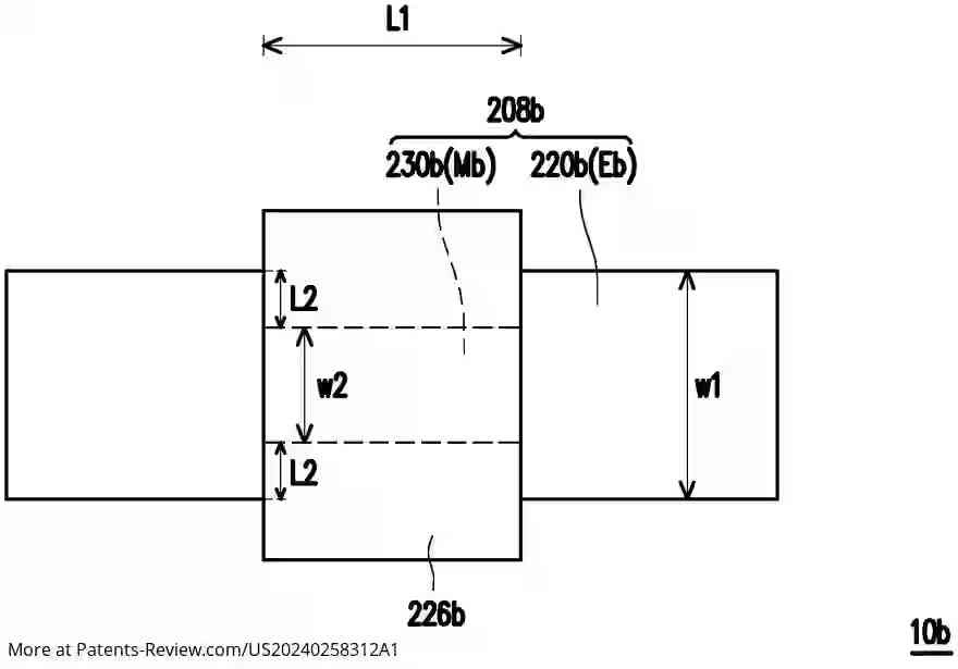
A semiconductor device is designed with a substrate that features two distinct regions, each containing semiconductor fins. The first region includes at least one first semiconductor fin with uniform width, while the second region consists of at least one second semiconductor fin that tapers in the middle. Insulators are placed on the substrate, sandwiching the fins, and gate stacks are positioned above portions of both types of fins. Additionally, source/drain (S/D) regions are incorporated to cover other sections of each fin.
Background on FinFET Technology
As semiconductor technology progresses, there is a shift from traditional planar CMOS devices to three-dimensional multi-gate structures like FinFETs. FinFETs utilize silicon fins encircled by gates to control the channel more effectively, offering enhanced electrical performance. This transition is crucial for achieving smaller device sizes while maintaining functionality and efficiency.
Manufacturing Process Details
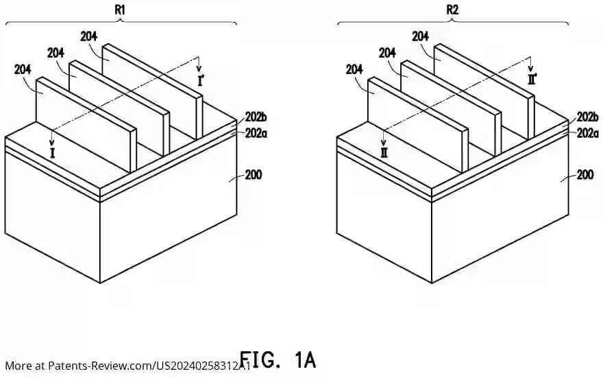
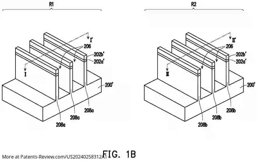
The manufacturing process involves various stages, including photolithography and etching techniques to create the desired fin structures on the substrate. A sacrificial layer is first applied and patterned, followed by the formation of spacers using self-aligned processes. Once the sacrificial layer is removed, the remaining spacers serve as a template for etching the fins.
Substrate Variations and Doping
The semiconductor substrate can be made from different materials such as silicon, germanium, or compound semiconductors. The substrate may also include doped regions to create either n-type or p-type FinFETs based on design requirements. Different doping concentrations can be applied in the first and second regions to support various functionalities in the semiconductor device.
Final Steps in Device Fabrication
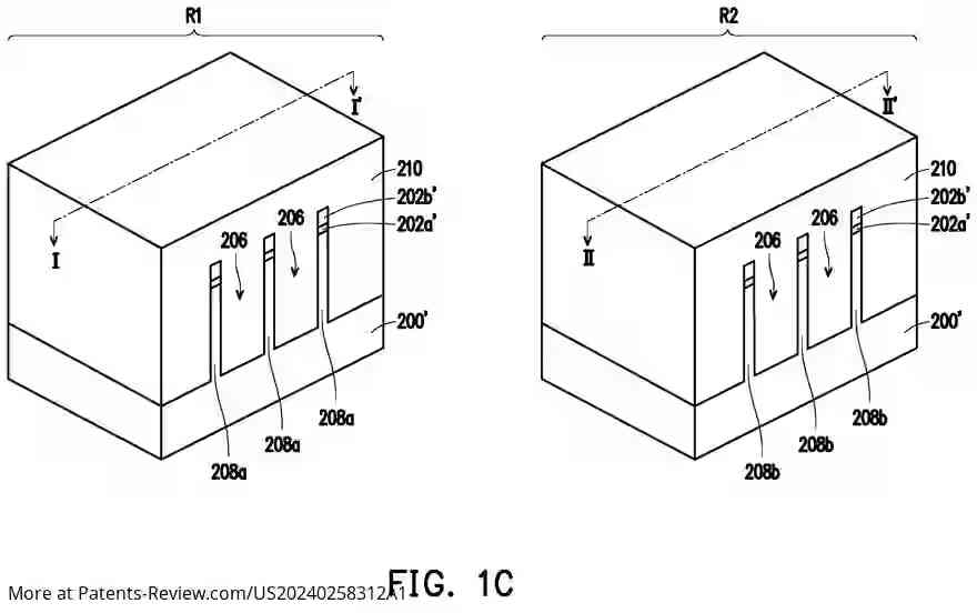
After forming trenches and fins through etching, a cleaning process is conducted to remove any native oxides from the substrate and fins. This ensures optimal conditions for subsequent processing steps. The resulting structure exhibits a combination of features tailored for high-performance applications, including ultra-low power operations in specific regions.