SEMICONDUCTOR DEVICE, FINFET DEVICE AND METHODS OF FORMING THE SAME
US20240258390
2024-08-01
Electricity
H01L29/41791
Inventors:
Assignee:
Applicant:
Drawings (4 of 24)


Smart overview of the Invention
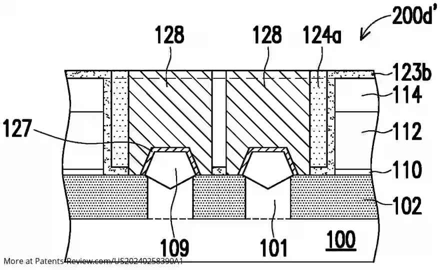
A semiconductor device comprises a substrate, a gate structure positioned on the substrate, a source/drain (S/D) region, and a contact. The S/D region is embedded within the substrate and located adjacent to the gate structure. Notably, the contact is designed to wrap around and connect with the S/D region, enhancing its connectivity and performance.
Importance of IC Evolution
The integrated circuit (IC) industry has seen rapid advancements, resulting in smaller and more complex circuits over generations. This scaling down process has led to increased functional density, meaning more interconnected devices can fit into a given chip area. While this enhances production efficiency and reduces costs, it simultaneously complicates the manufacturing process, necessitating innovations in IC fabrication techniques.
Embodiments of FinFET Device Formation
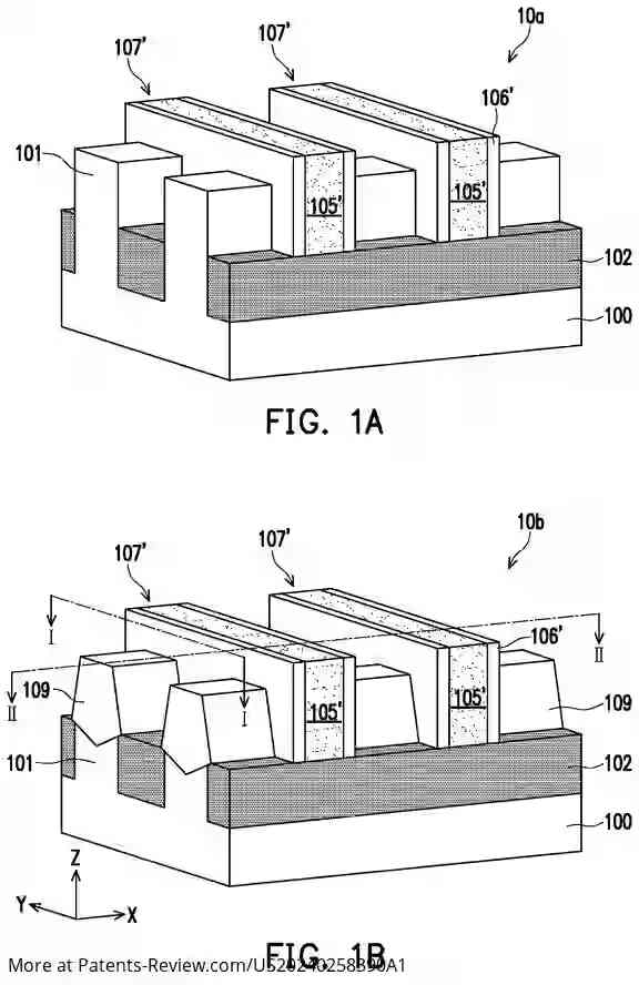
Various embodiments illustrate methods for forming a FinFET device. The fins of the device can be patterned through photolithography techniques, including double-patterning or multi-patterning processes. Such methods allow for creating patterns with smaller pitches than traditional direct photolithography, enhancing design capabilities and device performance.
Details on Substrate and Gate Structures
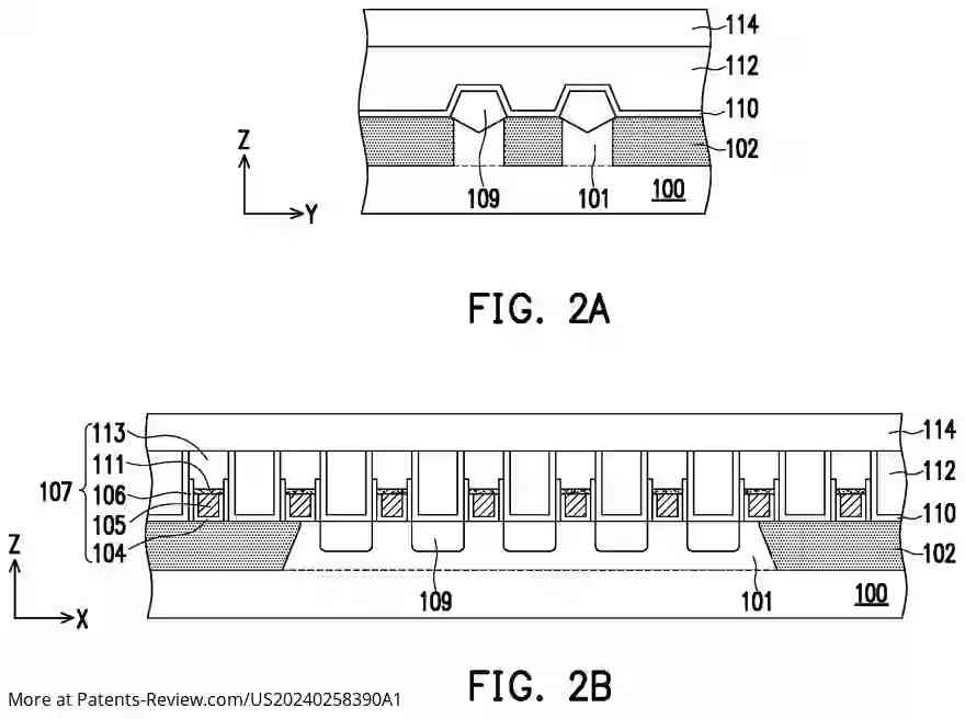
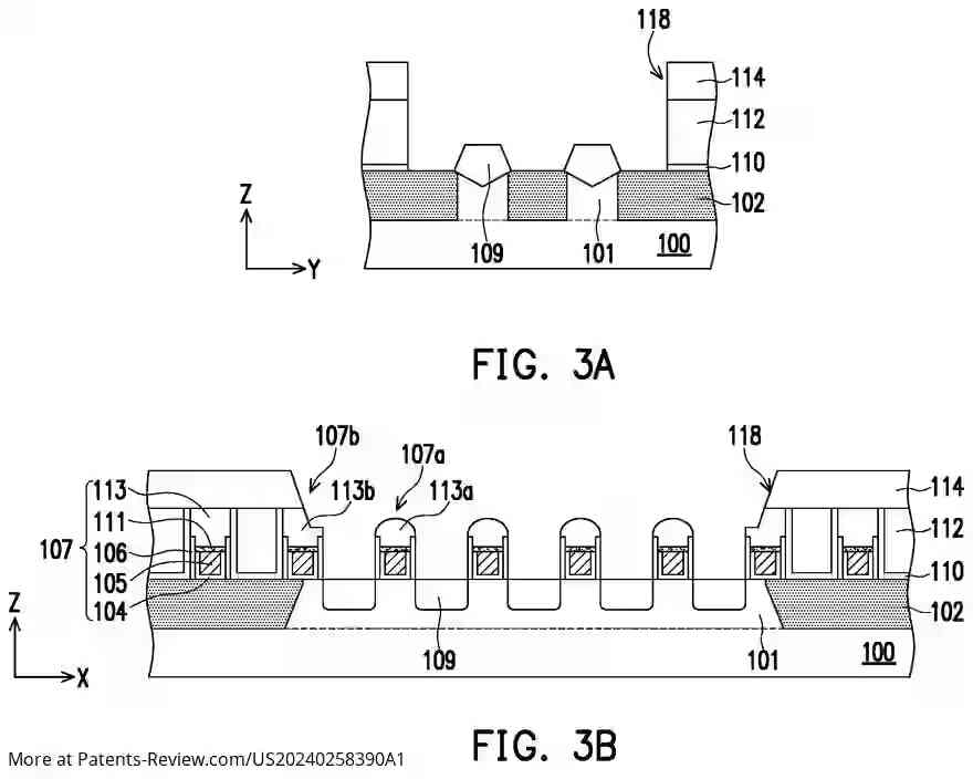
The semiconductor substrate can be made from various materials such as silicon or germanium and may include doped regions for specific device types. Gate structures formed on the substrate may initially be dummy structures that are later replaced with metallic gates. The formation process involves layering materials and utilizing photolithography and etching techniques to achieve precise configurations.
Source/Drain Region Formation
After establishing the gate structures, S/D regions are created on either side of them, with specific portions of the fins serving as channel regions. These S/D regions can include strained layers formed through selective epitaxial growth processes. Depending on the type of FinFET device (N-type or P-type), different materials are used for these strained layers to optimize performance characteristics.