INTEGRATED CIRCUIT AND FORMATION METHOD THEREOF
US20240258435
2024-08-01
Electricity
H01L29/78696
Inventor:
Assignee:
Applicant:
Drawings (4 of 29)


Smart overview of the Invention
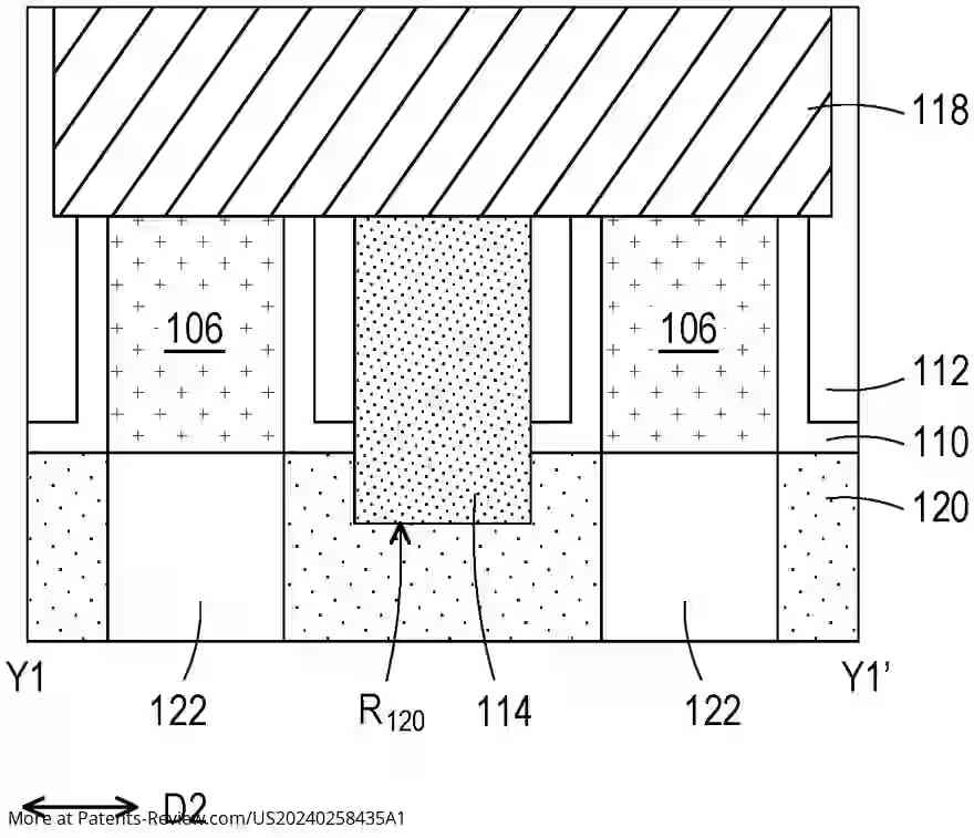
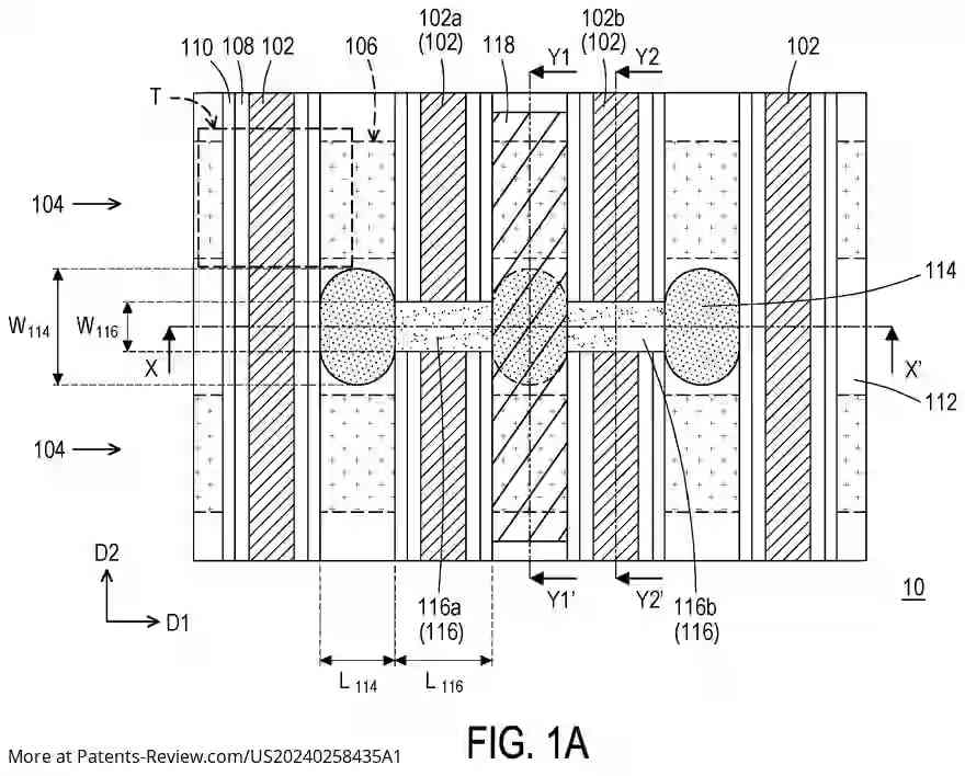
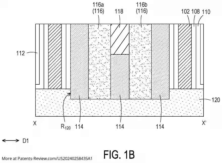
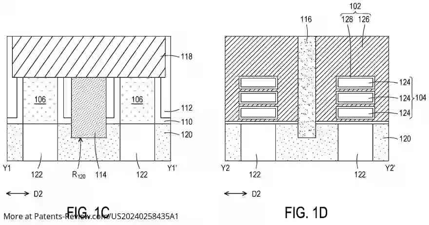
An innovative integrated circuit design incorporates multiple gate structures and channel structures, which penetrate laterally through the gate structures. The circuit features source/drain structures that are positioned between these gate structures, establishing lateral contact with the channel structures. An isolation wall is strategically placed between the source/drain structures, effectively segmenting the gate structures into distinct portions while maintaining a lateral contact structure that connects the source/drain structures without interruption.
Field Effect Transistors (FETs) Configuration
The integrated circuit utilizes field effect transistors (FETs) to facilitate various logic operations. Each FET consists of a gate terminal formed by the gate structure, with source and drain terminals located at either side. The design allows for the arrangement of N-type and P-type FETs along different channel structures, enabling the creation of diverse logic components. The spatial arrangement of these components is crucial for their functionality.
Isolation and Sidewall Structures
To ensure effective separation between gate and source/drain structures, sidewall spacers are employed along the edges of each gate structure. These spacers are complemented by an etching stop layer that provides additional isolation. The isolation wall further enhances this separation by cutting through adjacent gate structures, allowing for a more organized layout while preventing unwanted electrical interactions.
Interlayer Dielectric and Refilling Process
An interlayer dielectric fills gaps around the gate structures to create a planar surface suitable for interconnections. Openings within this dielectric are strategically formed and refilled with dielectric structures to enhance connectivity. These refilled structures are arranged in a manner that maintains proximity to both the gate and source/drain structures, ensuring efficient electrical pathways within the circuit.
Dimensional Considerations
The design emphasizes specific dimensional relationships between various components. The width of the isolation wall sections is intentionally narrower than that of the refilled dielectric structures, allowing for effective connectivity while maintaining structural integrity. The lengths of these components are calculated to optimize spacing and functionality, ensuring that all elements work harmoniously within the integrated circuit framework.