INTEGRATED CIRCUIT STRUCTURE AND MANUFACTURING METHOD THEREOF
US20240266218
2024-08-08
Electricity
H01L21/76897
Inventors:
Assignee:
Applicant:
Drawings (4 of 70)


Smart overview of the Invention
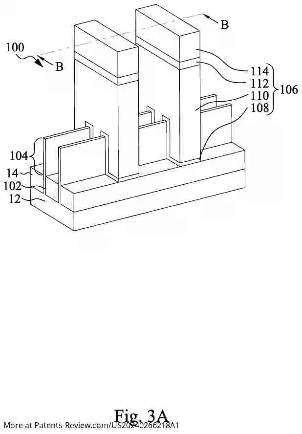
A semiconductor structure features a semiconductive fin, a gate structure, and multiple source/drain regions. The gate structure spans across the fin, while the source/drain regions are positioned on either side of the gate. Two types of dielectric caps are included: an un-oxidized dielectric cap on top of the gate structure and an oxidized dielectric cap above it.
Background of Integrated Circuits
Advancements in integrated circuit (IC) materials and designs have led to increasingly smaller and more complex circuits. As IC technology evolves, functional density increases, allowing for more interconnected devices within a given chip area. This trend of scaling down components generally improves production efficiency and reduces costs.
Manufacturing Process Details
The patent describes various methods for implementing the semiconductor structure, including photolithography techniques. These methods enable the creation of intricate patterns necessary for modern ICs. For instance, fins can be patterned using double or multi-patterning processes, which combine photolithography with self-aligned techniques to achieve finer pitches than single photolithography alone.
Formation of Source/Drain Contacts
After completing front-end-of-line (FEOL) processing for transistor fabrication, source/drain contacts are established over the designated regions. This involves forming source/drain vias to connect these contacts to interconnect metal lines. Specific layers such as interlayer dielectric (ILD) and middle contact etch stop layer (MCESL) are utilized to prevent over-etching during the manufacturing process, thereby reducing leakage current risks.
Variations in Fin Materials
The fins can be composed of various semiconductor materials depending on their function in the circuit. For n-type transistors, materials like Si or III-V compounds may be used, while p-type transistors could utilize materials such as SiGe or other suitable semiconductors. The design allows for flexibility in material choice to optimize performance based on specific electronic requirements.