METHOD OF MANUFACTURING A SEMICONDUCTOR DEVICE AND A SEMICONDUCTOR DEVICE
US20240274649
2024-08-15
Electricity
H01L28/20
Inventors:
Assignee:
Applicant:
Drawings (4 of 18)


Smart overview of the Invention
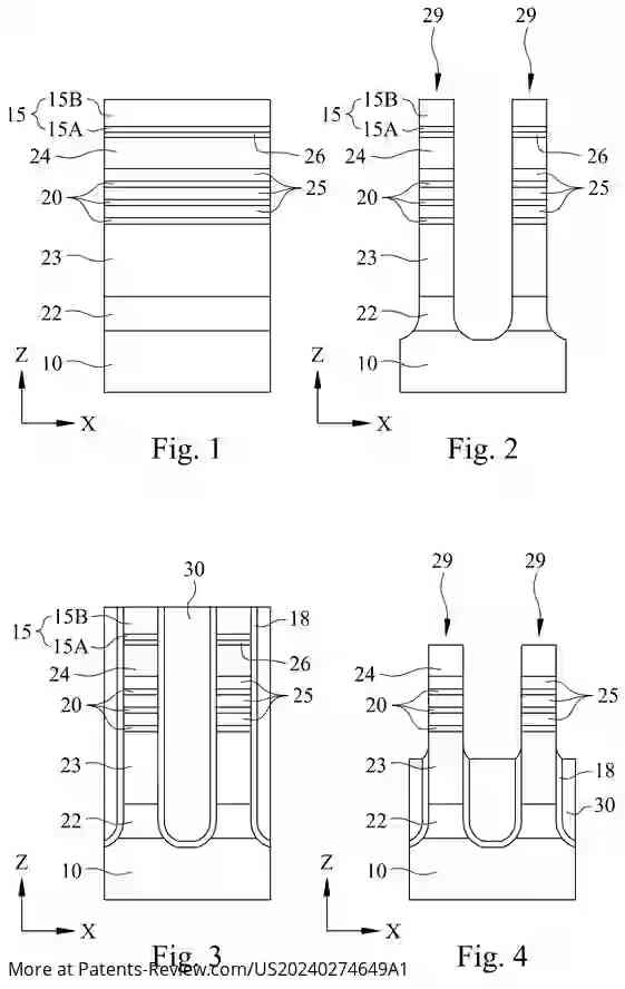
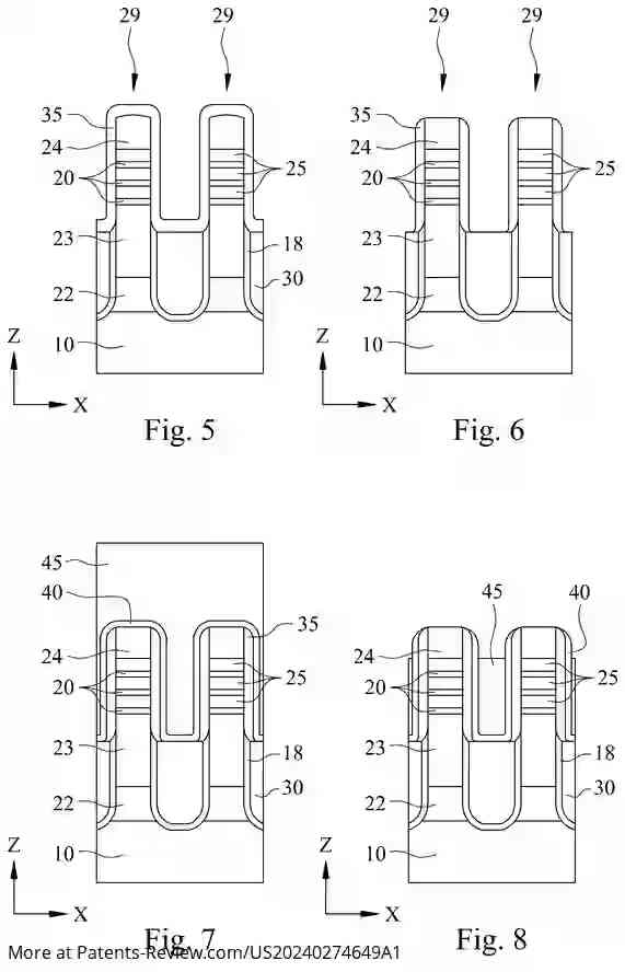
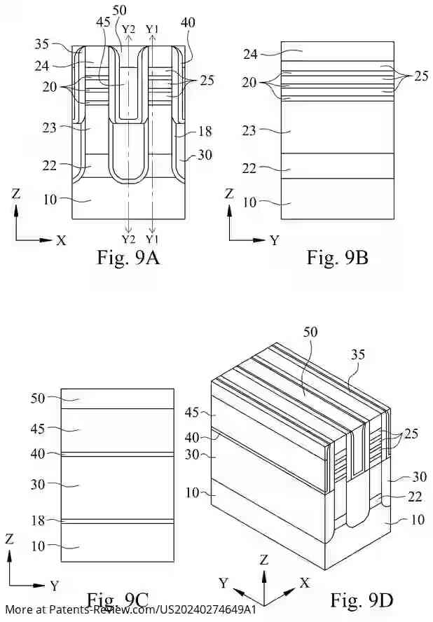
A semiconductor device is manufactured using a method that involves creating a fin structure made up of alternating layers of first and second semiconductor materials. This structure is placed on a bottom fin structure and covered by a hard mask layer. Following this, an isolation insulating layer is added, along with a sacrificial cladding layer that coats the sidewalls of the hard mask and stacked layers. The process continues with the formation of multiple dielectric layers, which are subsequently recessed and shaped to create a trench, ultimately leading to the formation of a wall fin structure.
Advancements in Fin FET and GAA FET Technologies
The development of three-dimensional transistor designs, such as Fin FET and gate-all-around (GAA) FET, has emerged in response to challenges faced by the semiconductor industry as it moves towards smaller technology nodes. Fin FETs utilize a gate electrode that wraps around three sides of the channel region, while GAA FETs fully encase the channel, allowing for better control over current flow and improved performance. As dimensions shrink below 10-15 nm, enhancements in GAA FET design are crucial for continued progress.
Importance of Epitaxial Source/Drain Structures
The performance of field effect transistors (FETs) is significantly influenced by the shape of the epitaxial source/drain structures. Recessing the source/drain regions before forming these layers ensures that their shape is well-defined. However, issues can arise when adjacent fin structures are too close together, causing unwanted merging of epitaxial layers. To mitigate this, a wall fin structure is introduced to separate these layers physically and electrically, enhancing device performance by optimizing the source/drain shape.
Details of Semiconductor Layer Formation
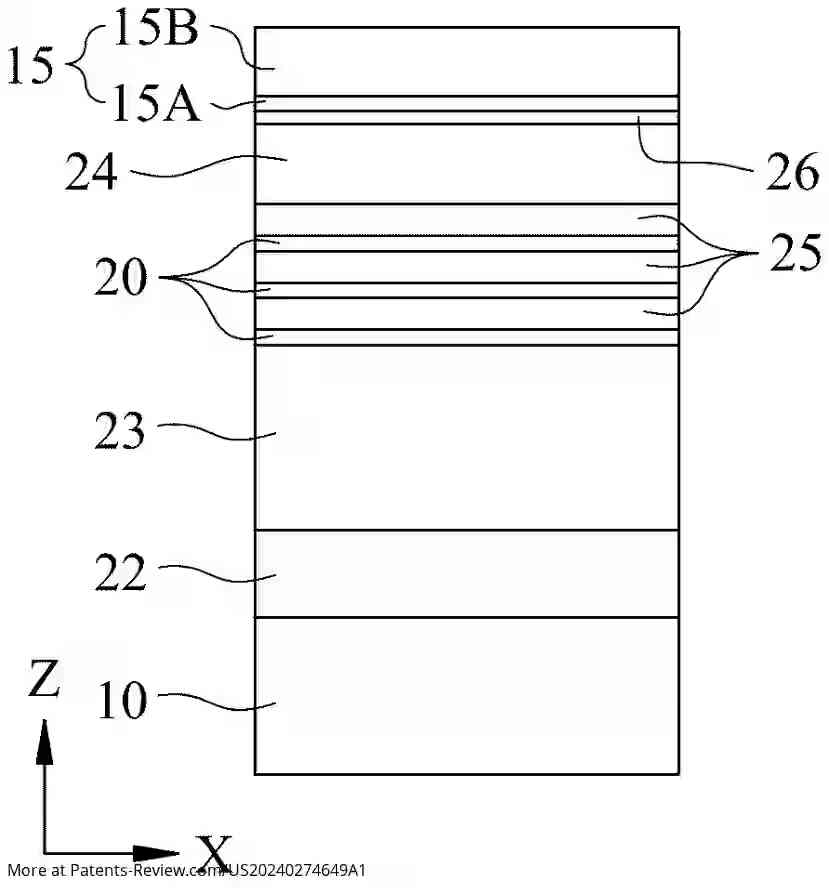
The manufacturing process begins with the epitaxial formation of various semiconductor layers on a substrate. The first bottom semiconductor layer is typically made from materials like SiGe, while the second layer may be Si or another variation with lower germanium content. Subsequent layers are formed alternately, ensuring different lattice constants are utilized to enhance performance. A top semiconductor layer may also be added to further improve device characteristics.
Utilization of Hard Mask Layers
A hard mask layer composed of insulating or amorphous semiconductor materials is applied over the top semiconductor layer to aid in the shaping process during manufacturing. This layer consists of multiple components that offer varying thicknesses and properties. By employing these hard masks effectively, manufacturers can ensure better control during subsequent processes such as chemical mechanical polishing, ultimately leading to higher quality semiconductor devices.