SEMICONDUCTOR DEVICE STRUCTURE AND METHOD FOR FORMING THE SAME
US20240274717
2024-08-15
Electricity
H01L29/785
Inventors:
Assignee:
Applicant:
Drawings (4 of 32)


Smart overview of the Invention
A semiconductor device structure is designed to enhance the performance and efficiency of integrated circuits. It incorporates a series of nanowire structures positioned over a channel region of a semiconductor fin structure, alongside a source/drain feature situated within a designated source/drain region. A dielectric fin structure is also included, which is intentionally spaced apart from both the source/drain feature and the semiconductor fin structure, ensuring optimized electrical characteristics.
Importance of Miniaturization in Electronics
The electronics industry is increasingly focused on producing smaller and faster devices that can handle more complex functions. This trend has driven semiconductor manufacturers to reduce the dimensions of integrated circuits while improving performance and lowering costs. However, this miniaturization has complicated manufacturing processes, necessitating advancements in semiconductor technology to maintain efficiency and effectiveness.
Advancements with Multi-Gate Devices
Multi-gate devices, particularly gate-all-around (GAA) transistors, have emerged as a solution to improve gate control and reduce OFF-state current. These devices allow for enhanced channel access by wrapping the gate structure around the channel on multiple sides. GAA transistors are compatible with traditional CMOS processes, enabling aggressive scaling while mitigating short-channel effects, although challenges remain in their fabrication integration.
Methodology for Structure Formation
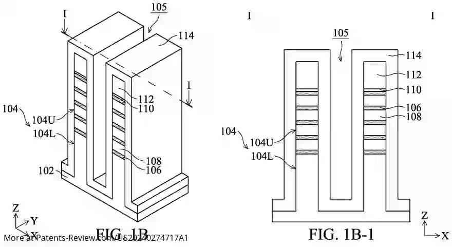
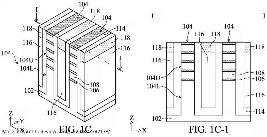
The formation of the semiconductor device structure involves various steps, including photolithography and self-aligned processes. For instance, a sacrificial layer is applied and patterned using photolithography, followed by the formation of spacers through self-aligned methods. The removal of the sacrificial layer leaves behind spacers that help define the GAA structure, enhancing its performance by allowing for narrower source/drain features that reduce parasitic capacitance.
Material Composition and Layering Techniques
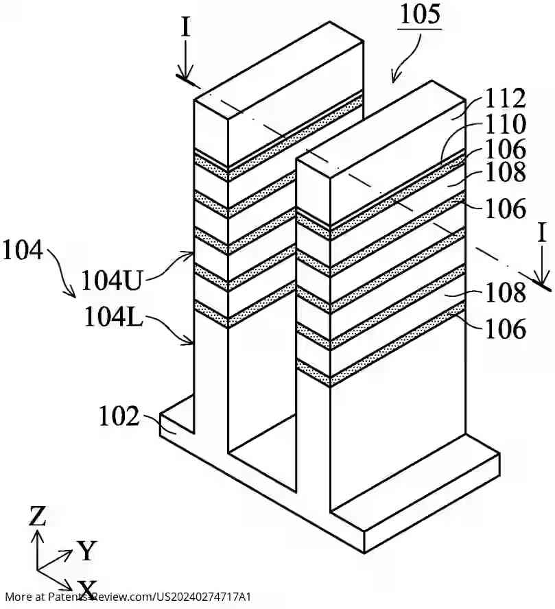
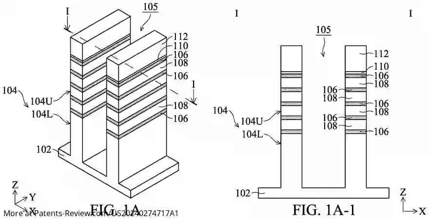
The semiconductor fin structures are constructed using a combination of different semiconductor materials stacked in layers. The first layers may consist of SiGe with varying germanium content, while the second layers typically comprise silicon. These materials are deposited using advanced techniques such as low-pressure chemical vapor deposition or epitaxial growth methods. This careful selection and layering of materials are crucial for optimizing device performance and achieving desired electrical characteristics.