MEMORY CELL, SEMICONDUCTOR DEVICE HAVING THE SAME, AND METHODS OF MANUFACTURING THE SAME
US20240284809
2024-08-22
Electricity
H10N70/231
Inventors:
Assignee:
Applicant:
Drawings (4 of 39)


Smart overview of the Invention
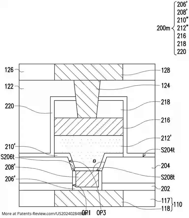
A memory cell consists of several key components: a bottom electrode, a storage element layer, a first buffer layer, and a top electrode. The storage element layer is positioned over the bottom electrode, while the first buffer layer is interposed between them. Notably, the thermal conductivity of the first buffer layer is lower than that of the storage element layer, which plays a crucial role in thermal management. The top electrode is placed above the storage element layer, effectively sandwiching it between the top electrode and the first buffer layer.
Background and Need for Alternatives
With ongoing advancements in semiconductor technology, there is an increasing demand for high integration density in electronic components. Flash memory, a popular nonvolatile memory type, faces challenges with scaling as device sizes shrink. As a result, alternatives such as phase change memory (PCM) are being explored. PCM offers advantages such as rapid read/write times and non-destructive reads, making it a promising candidate for future memory solutions.
Thermal Management Features
The inclusion of a thermal buffer layer within the memory cell design enhances thermal control. This layer's lower thermal conductivity compared to the storage element allows it to act as an insulator, reducing heat dissipation from the storage element after it has been heated. Consequently, this configuration enables efficient operation with lower input currents while maintaining effective switching performance.
Device Density Improvement
Utilizing a small input current for operation allows for increased device density within a given area. This design approach helps to meet stringent voltage and current requirements without compromising performance. By optimizing thermal management and reducing operational currents, the memory cell can be integrated more densely into semiconductor devices.
Manufacturing Process Overview
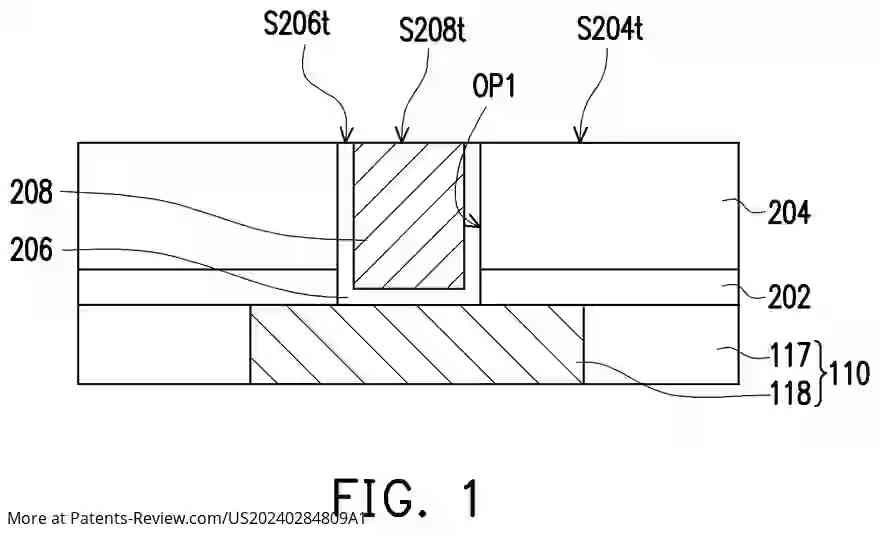
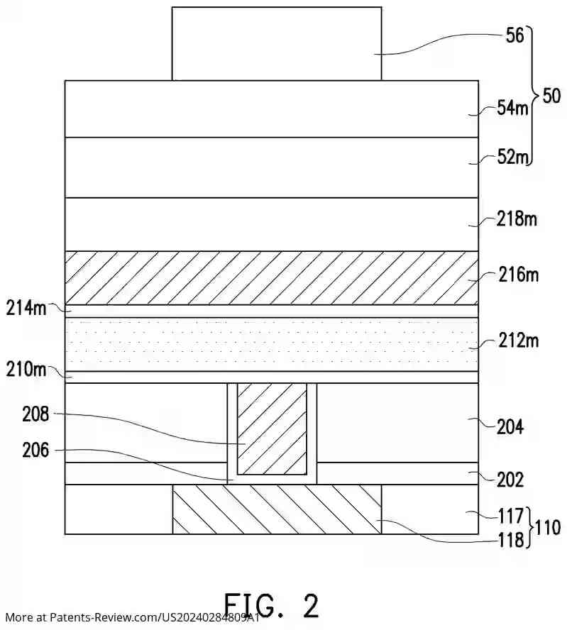
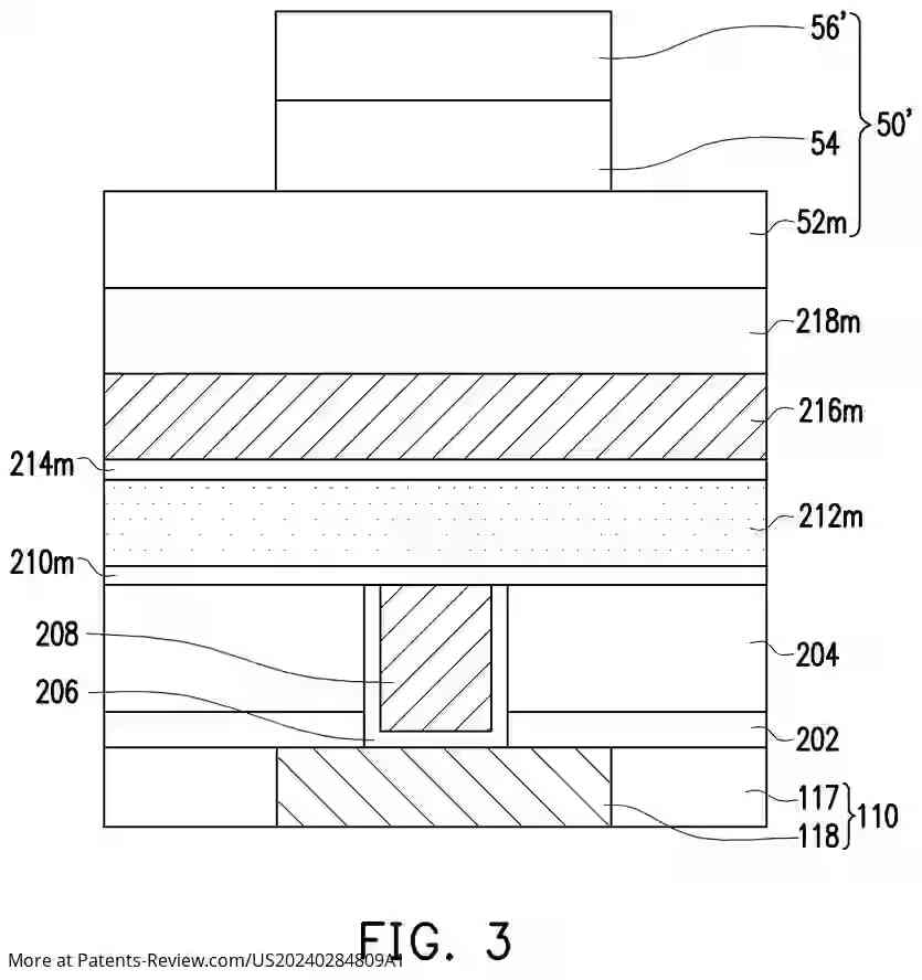
The manufacturing process involves several steps to create the semiconductor device featuring the memory cell. Initially, an interconnect structure is established, followed by stacking dielectric layers and forming the bottom electrode within an opening that connects to conductive layers. Additional barrier layers may be employed to prevent diffusion during fabrication. This systematic approach ensures that each component of the memory cell is precisely positioned for optimal functionality.