SEMICONDUCTOR STRUCTURE AND METHOD FOR FORMING THE SAME
US20240290863
2024-08-29
Electricity
H01L29/66545
Inventors:
Assignee:
Applicant:
Drawings (4 of 21)


Smart overview of the Invention
A semiconductor structure is designed with a vertical channel layer, which is flanked by both a top and bottom source/drain (S/D) structure. The channel layer is enveloped by a gate structure, enhancing its performance. Additionally, a top inner spacer layer sits atop the gate structure, ensuring that the top surface of the channel layer is positioned higher than the bottom surface of the spacer layer.
Manufacturing Methods
The patent outlines various methods for manufacturing these semiconductor structures, emphasizing flexibility in design. Techniques such as photolithography, including double-patterning and multi-patterning processes, are utilized to create intricate patterns with smaller pitches than traditional methods allow. This involves using sacrificial layers and self-aligned processes to achieve precise structures.
Material Composition
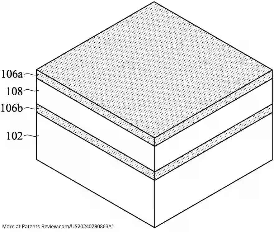
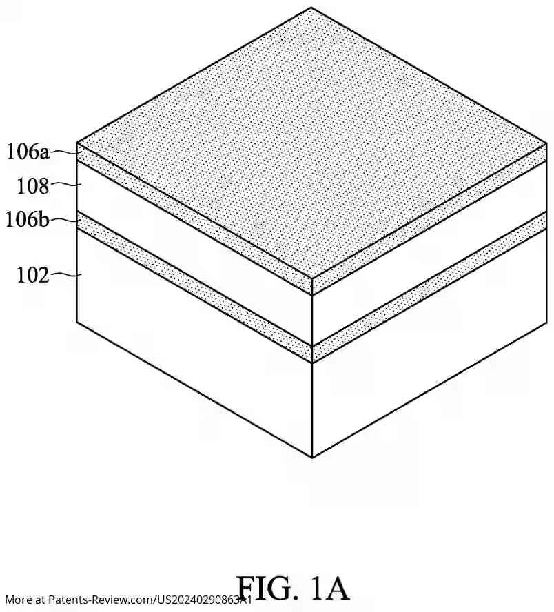
The semiconductor layers can consist of different materials stacked alternately over a substrate, which may be silicon or other semiconductor materials. These materials can include SiGe for the first layers and silicon for the channel layer. The formation processes mentioned include low-pressure chemical vapor deposition and epitaxial growth techniques.
Structural Features
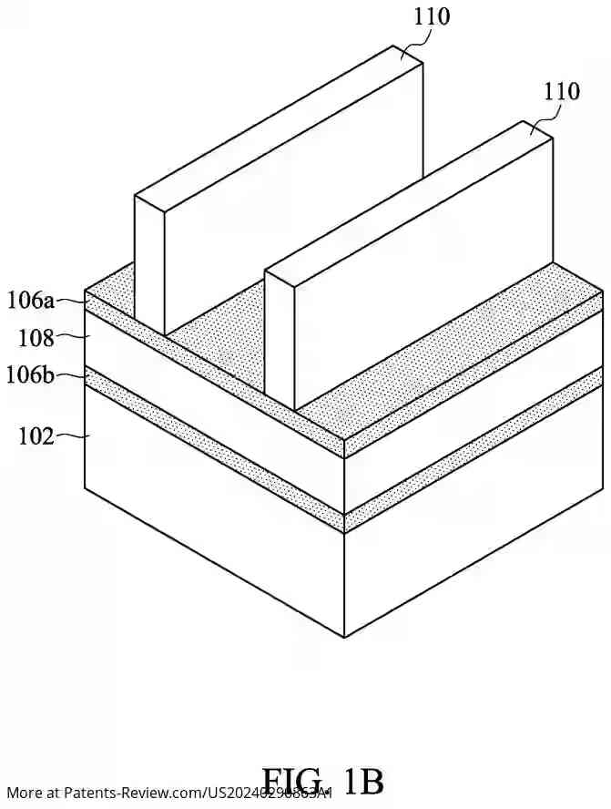
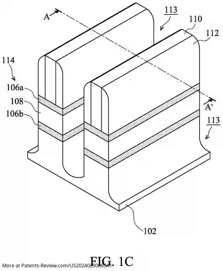
After forming the semiconductor material stack, a mask layer is applied and patterned to guide further etching processes. Spacer layers are created alongside these masks to define fin structures. The resulting fin structures have notches formed through selective etching, leading to a unique design that enhances the performance characteristics of the semiconductor structure.
Process Variations
Different embodiments are described to illustrate variations in manufacturing processes. These include adjustments in etching techniques that allow for precise control over the dimensions of layers, ensuring that notches formed between layers have specific depth and thickness ratios. This level of detail in manufacturing contributes to improved overall performance of the resulting semiconductor devices.