METHOD OF REDUCING UNDESIRED LIGHT INFLUENCE IN EXTREME ULTRAVIOLET EXPOSURE
US20240295820
2024-09-05
Physics
G03F7/11
Inventors:
Assignee:
Applicant:
Drawings (4 of 9)


Smart overview of the Invention
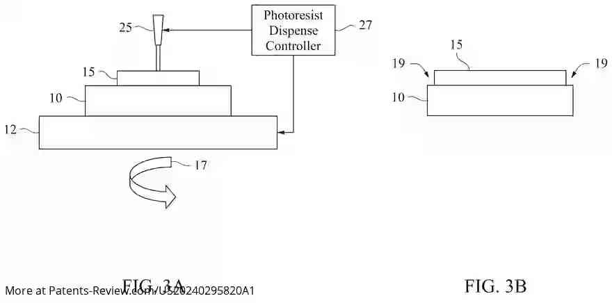
A method is described for generating layout patterns on a substrate using a photoresist layer. This involves placing a transparent top layer over the photoresist, which allows extreme ultraviolet (EUV) radiation to pass through while blocking deep ultraviolet (DUV) radiation. The process includes irradiating the photoresist with radiation from an EUV source, ensuring that only the desired wavelengths affect the photoresist layer.
Challenges in IC Design
In integrated circuit (IC) design, creating precise layout patterns is crucial. These patterns are transferred onto photoresist layers via lithography processes using EUV radiation. However, the EUV light source can also emit out-of-band DUV wavelengths that may interfere with imaging. This interference can lead to blurred patterns and degraded critical dimension (CD) uniformity, which are essential for the performance of the IC.
Impact of DUV Radiation
The presence of out-of-band DUV radiation poses significant challenges during the imaging process. When using reflective masks, this unwanted radiation can be reflected back towards the photoresist, adding an undesirable bias to the exposure energy. As a result, this bias can adversely affect CD uniformity, particularly for features near the resolution limit of the EUV source.
Implementation of Spectral Filters
To mitigate the effects of out-of-band DUV radiation, a thin spectral filter layer can be applied over the substrate. This layer absorbs DUV wavelengths while allowing EUV radiation to reach the photoresist. The thickness of this filter is tailored to effectively block specific DUV wavelengths, enhancing image sharpness and preserving pattern integrity on the photoresist layer.
System Configuration
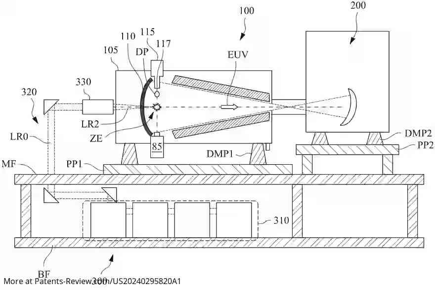
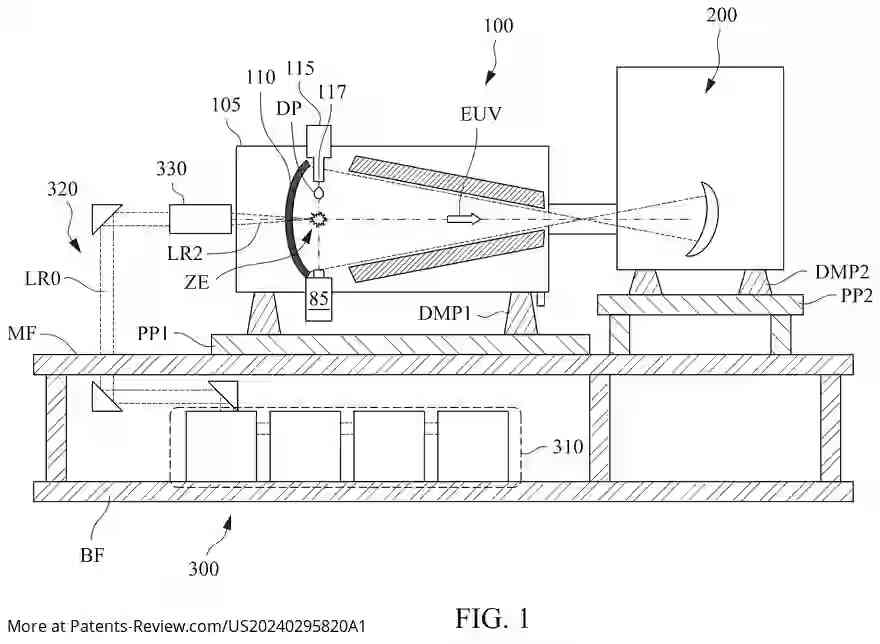
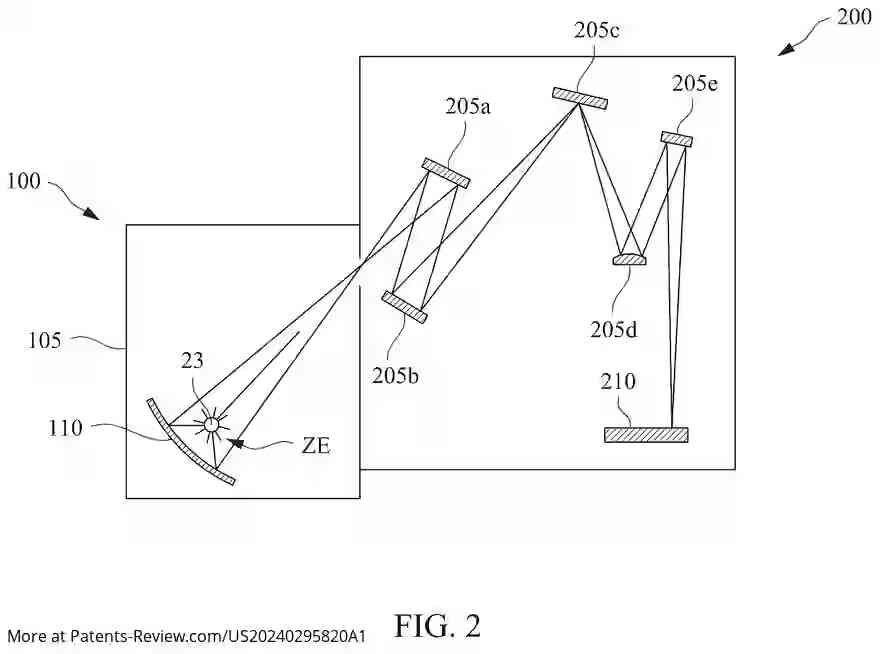
The described method is implemented within an EUV lithography system that includes a laser-produced plasma (LPP) EUV radiation source and an exposure device. This configuration is designed to optimize exposure by generating EUV light within a specific wavelength range while minimizing interference from unwanted DUV radiation, thus improving overall pattern quality on semiconductor wafers.