SEMICONDUCTOR DEVICES WITH ELECTRICAL FUSES AND METHODS OF FABRICATING THE SAME
US20240297115
2024-09-05
Electricity
H01L23/5256
Inventors:
Assignee:
Applicant:
Drawings (4 of 18)


Smart overview of the Invention
A semiconductor structure comprises a substrate with two surfaces. On the first surface, a semiconductor device is positioned, while a metallization layer is located on the second surface. Two conductive vias, the first and second, are connected in parallel to the metallization layer and extend from the second surface to the first. An electrical fuse is situated above the semiconductor device and connects to both conductive vias, enabling its functionality within the device.
Importance of Electrical Fuses
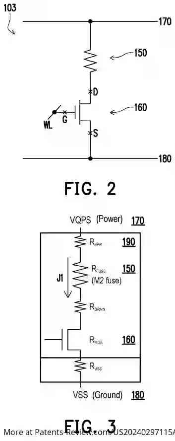
Electrical fuses (eFuses) are critical components in integrated circuit (IC) chips, allowing for reprogramming and performance tuning. When a part of an IC fails, an eFuse can be activated to modify behavior or switch to backup systems. Typically, eFuse cells utilize a one-transistor-one-resistor (1T1R) architecture, where a transistor is linked to a resistor. While existing eFuse designs serve their purpose, they have limitations that necessitate improvements.
Challenges with Current eFuse Implementations
As technology evolves, integrating eFuses into ICs presents challenges due to smaller feature sizes. When components of an eFuse are placed on the front side of an IC chip and powered from the back side, the small diameter of vias can increase resistance. This resistance can hinder sufficient current flow necessary for programming the eFuse, making it difficult to achieve desired functionality in ICs.
Innovative Solutions for Enhanced Performance
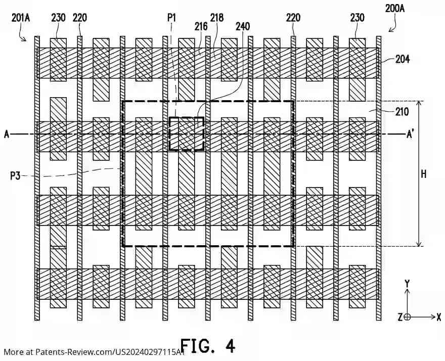
The proposed semiconductor device features an eFuse cell connected to a backside power source through multiple low-resistance vias. This configuration aims to enhance current delivery to the fuse element, ensuring it can meet programming requirements effectively. Various embodiments illustrate different arrangements and components that simplify implementation while improving performance.
Configuration of eFuse Cells
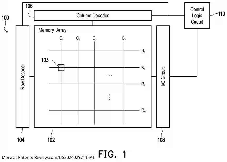
The eFuse cell is typically designed using a 1T1R configuration, consisting of a fuse resistor and an access transistor arranged in series. The access transistor is activated to allow programming or reading of the fuse resistor. Both components are formed on the same side of the substrate during processing phases, ensuring efficient integration within the semiconductor structure while maintaining optimal performance characteristics.