SEMICONDUCTOR DEVICE AND MANUFACTURING METHOD THEREOF
US20240297252
2024-09-05
Electricity
H01L29/7848
Inventors:
Assignee:
Applicant:
Drawings (4 of 14)


Smart overview of the Invention
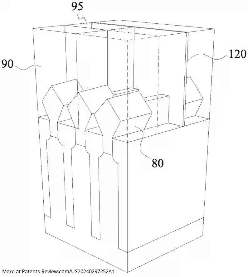
A fin field effect transistor (Fin FET) device features a fin structure that extends in one direction, protruding from an isolation insulating layer situated above a substrate. This fin structure comprises multiple layers: a well layer, an oxide layer, and a channel layer. A gate structure covers part of the fin and extends perpendicularly to the fin's direction. The Fin FET device also includes a source and a drain, each equipped with a stressor layer that enhances the performance of the channel layer by applying stress.
Advancements in Semiconductor Technology
The semiconductor industry has evolved towards nanometer technology to achieve higher device density and improved performance. As part of this evolution, three-dimensional designs like Fin FETs have emerged. These devices utilize high aspect ratio semiconductor fins, allowing for enhanced control over channel and source/drain regions. The increased surface area afforded by this design contributes to faster and more reliable transistor performance.
Manufacturing Process of Fin FETs
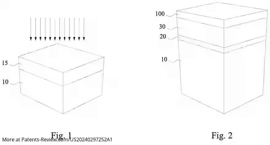
- The process begins with the implantation of impurity ions into a silicon substrate to create a well region, preventing punch-through effects.
- Subsequent layers are grown epitaxially, including first layers made of materials such as SiGe and second layers of silicon.
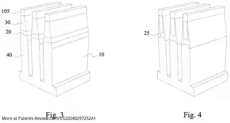
- A mask layer is applied and patterned to facilitate etching into fin structures using dry or wet methods.
Oxidation and Isolation Layer Formation
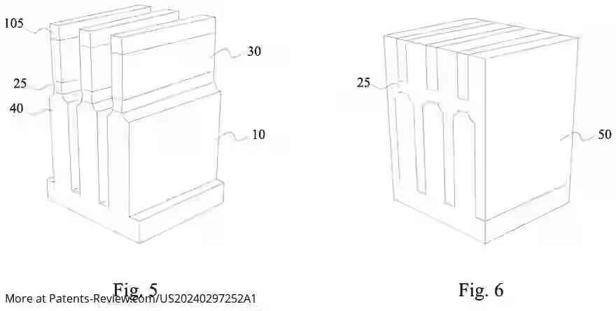
After etching, the first epitaxial layer undergoes selective oxidation to form an oxide layer. This is achieved through wet oxidation processes that take advantage of the differing oxidation rates of SiGe and silicon. Following this, portions of the oxide layer are removed, and an isolation insulating layer is formed using various deposition techniques to ensure proper insulation between components.
Material Composition and Layer Characteristics
The isolation insulating layer can comprise multiple materials such as silicon oxide or silicon nitride, often deposited using low-pressure chemical vapor deposition (LPCVD) or other advanced techniques. The manufacturing process allows for variations in thickness and composition depending on desired properties, ensuring that the resulting Fin FET device meets specific performance criteria essential for modern semiconductor applications.