SENSOR, IMAGE SENSOR, DISPLAY PANEL, AND DEVICE
US20250271298
2025-08-28
Physics
G01J1/44
Inventors:
Assignee:
Applicant:
Drawings (4 of 16)


Smart overview of the Invention
The patent describes a sensor featuring an anode, a cathode, and an organic photoelectric conversion layer positioned between them. This layer consists of both p-type and n-type semiconductors and incorporates a first singlet fission material. A key aspect of this design is that the LUMO energy level of the singlet fission material is equal to or deeper than that of the n-type semiconductor. Such configuration aims to enhance the sensor's sensitivity and integration capabilities.
Technical Background
Photoelectric conversion devices, which convert absorbed light into electrical signals, are essential in various optical applications. Traditional materials like silicon often require additional components, such as color filters, to achieve wavelength selectivity. The demand for higher resolution in sensors necessitates smaller pixel sizes, which can limit silicon's absorption efficiency. The proposed sensor addresses these limitations by utilizing organic materials that improve sensitivity and integration.
Innovative Features
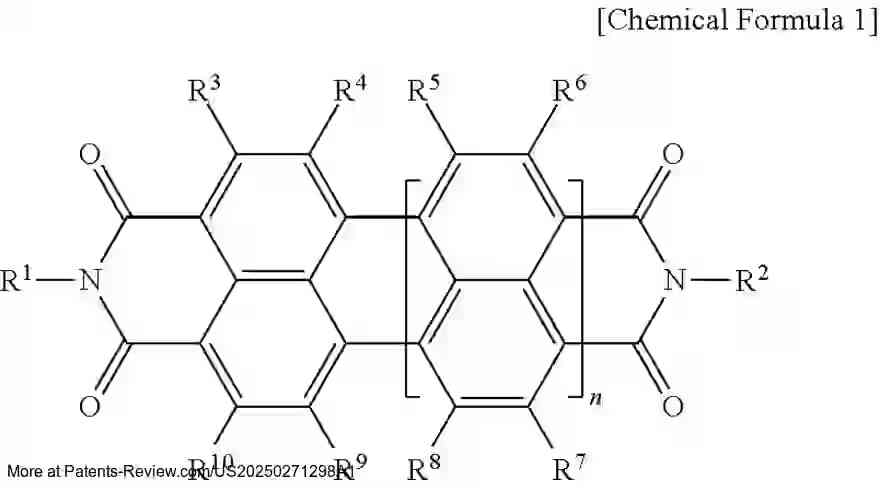
This sensor introduces a first organic auxiliary layer between the cathode and the photoelectric conversion layer. The singlet fission material within this layer is tailored to absorb specific wavelengths, potentially covering blue, green, red, and infrared spectrums. The device architecture includes additional layers like an electron auxiliary layer and a second organic auxiliary layer, each contributing to optimized energy levels that enhance efficiency.
Applications
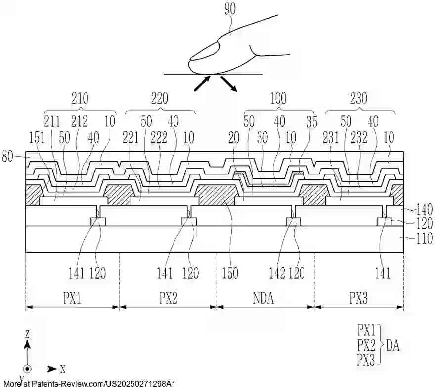
The sensor can be integrated into image sensors and display panels. Image sensors may include multiple photodiodes and color filters to manage different wavelength spectrums effectively, enhancing image quality and device functionality. Display panels can incorporate light-emitting elements for various colors alongside the sensor array, allowing for versatile applications in consumer electronics.
Advantages
The proposed design improves both external and internal quantum efficiency while maintaining compact sensor dimensions. This approach allows for increased sensitivity without compromising on size or integration density. The use of singlet fission materials ensures that the device remains efficient across different wavelength spectrums, making it suitable for advanced imaging and display technologies.