OPTICAL CONNECTOR, OPTICAL PIGTAIL, OPTICAL PATCH CORD, AND OPTICAL COMMUNICATION DEVICE AND SYSTEM
US20250271625
2025-08-28
Physics
G02B6/3885
Inventors:
Assignee:
Applicant:
Drawings (4 of 25)


Smart overview of the Invention
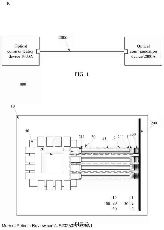
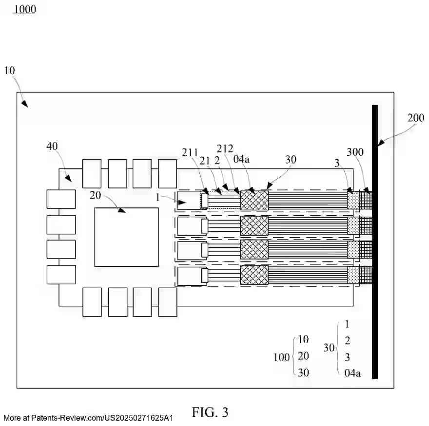
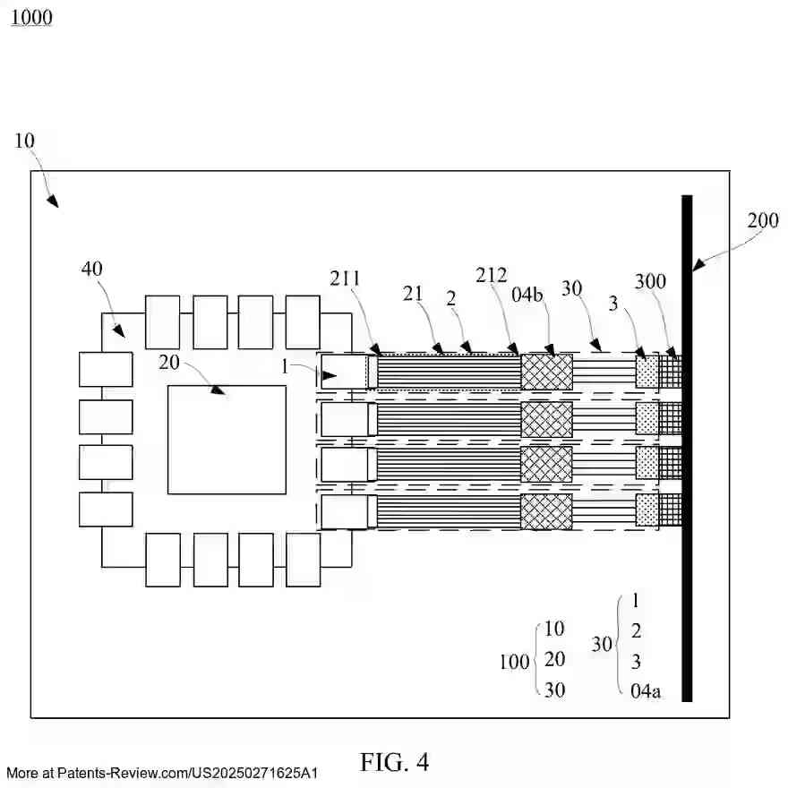
The patent application presents an innovative optical connector that integrates multiple functionalities within a single device, aiming to enhance optical communication technologies. The connector features an optical waveguide device and a fastening structure, enabling operations like splitting, combining, demultiplexing, multiplexing, and more, without altering the size of the existing connectors. This integration reduces the size of optical modules and minimizes the board area they occupy.
Technical Field
The invention is relevant to optical communication technologies, particularly in environments requiring large capacity and low latency such as switches, AI clusters, and high-performance computing clusters. The evolution from traditional pluggable optical modules to advanced configurations like on-board optics (OBO) and co-package optics (CPO) necessitates advancements in optical connectors to handle increased transmission rates and channel quantities.
Problem Addressed
Current optical modules face challenges with space consumption due to the need for independent converters and multiplexers/demultiplexers. These components, essential for technologies like space division multiplexing (SDM) and wavelength division multiplexing (WDM), require additional space on the mainboard. This invention addresses these issues by integrating these functions into a single optical connector.
Key Features
- Optical Waveguide Device: Performs multiple functions such as multi-core to single-core conversion and optical power adjustment.
- Fastening Structure: Ensures secure alignment and connection of the optical transmission medium with the waveguide device.
- Material Flexibility: Constructed from materials like glass, silicon dioxide, or high polymers to meet diverse transmission needs.
- Compact Design: Eliminates the need for separate converters or multiplexers, reducing module size and enhancing integration.
Implementation Variations
The fastening structure can take various forms such as clamping plates or positioning grooves to accommodate different installation requirements. Additionally, a ferrule may be included for mechanical protection. The design supports both single-layer and multi-layer structures to adapt to specific signal transmission scenarios. The connector's versatility allows for seamless integration into existing systems while providing improved efficiency and reduced spatial demands.